June 29, 2020 - by Oliver Morsch
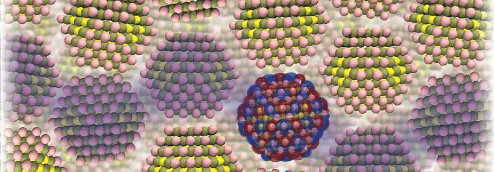
A few years ago, we were introduced to TV screens featuring QLED technology that produces brilliant colours. The “Q” here stands for “quantum dot”. Quantum dots are crystals of a semiconductor material only a few nanometres in size that consist of a couple of thousand atoms. Those nanocrystals are so tiny that the electrons in them can only take on certain well-defined quantum mechanical energy levels. As a consequence, when quantum dots are illuminated by the backlight of a TV, light of a particular colour is emitted by quantum jumps between those levels.
In next generation QLED TVs, the hope is to use electricity to make the quantum dots glow on their own instead of needing a backlight. Up to now, however, the theoretical understanding of how electrical current moves through a thin film of nanocrystals was lacking. A team of researchers from the Department for Information Technology and Electrical Engineering of ETH Zurich led by Vanessa Wood have now closed that gap, as they report in the scientific journal Nature Communications.
Spring mattress vs table top
The theory of how electric current moves in semiconductors that aren’t nanosized has been known for more than ninety years and software tools exist to model their behaviour. Industry can control the electronic properties of semiconductors by deliberately adding impurity atoms (doping), which changes the number of free charge carriers (electrons). By contrast, semiconductors consisting of many small nanocrystal quantum dots cannot be treated with those methods.
In nanocrystals, adding impurity atoms doesn’t necessarily lead to free charge carriers. Furthermore, free charges don’t behave in the same way. “Charge carriers in a normal semiconductors move like bowling balls rolling on a smooth table top, whereas in a nanocrystal material they act like bowling balls on a soft mattress, sinking in and deforming it”, Wood illustrates the problem.
Demanding modelling
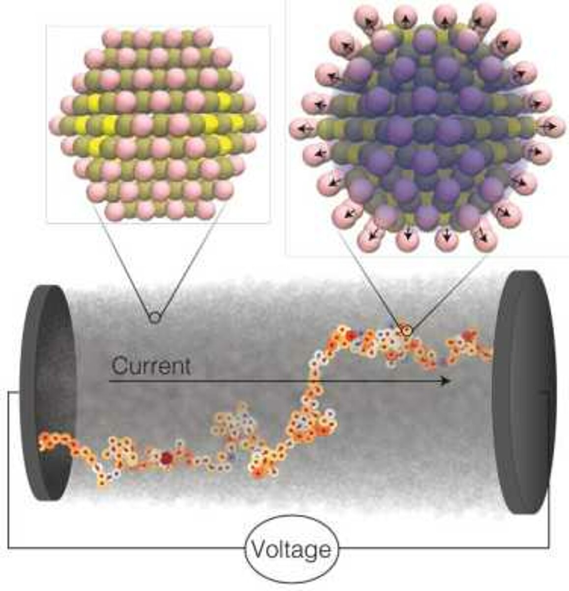
For the theoretical modelling this means that the atoms in the crystal lattice of the nanocrystal semiconductor cannot simply be looked at as stationary points, which is what is usually done with normal semiconductors. “Rather, we had to mathematically describe every one of the several hundred thousand atoms in the many nanocrystals of the material, and how each atom interacts with charge carriers”, explains Nuri Yazdani, who worked in Wood’s research group as a PhD student and is first author of the recently published study.
Using the Swiss Supercomputing Centre CSCS in Lugano, Yazdani ran a complex code in which all the details of the problem – the motion of the electrons and the atoms as well as the interactions between them – were taken into account. “In particular, we wanted to understand how charge carriers move between the single nanocrystals and why they get ‘trapped’ and can’t go on”, says Yazdani.
The results of those computer simulations were extremely revealing. It turned out that the determining factor in how a material composed of many nanocrystals conducts electrical current are the tiniest deformations of the crystals, only a few thousandths of a nanometer, that lead to a huge change in electrostatic energy. When charge deforms the material around it, this is known as a polaron, and Yazdani’s simulations show that current flows through polarons hopping from one nanocrystal to the next.
One model explains all
The model explains how the electronic properties of the nanocrystal-based semiconductors are changed by varying the size of the nanocrystals and how they pack in the film. To test the predictions of their simulations, the team produced thin films of nanocrystals in the laboratory and measured the electric response for different applied voltages and temperatures. In those experiments, they created free electrons at one end of the material using a short laser pulse and then observed when they arrived at the other end. The result: for each of the several hundred different tests, the computer simulation perfectly predicted the electrical properties.
“After eight years of intense work, we have now created a model that can finally quantitatively explain not just our experiments, but also those of many other research groups over the past years”, says Wood. “Such a model will enable researchers and engineers in the future to calculate the properties of a nanocrystal semiconductor even before it is produced.” This should make it possible to optimize such materials for particular applications. “So far, this had to be done by trial and error”, Wood adds.
Using the results of the ETH researchers, in the future useful semiconductors could be developed from nanocrystal materials for various applications in sensors, lasers or LEDs – also for TV screens. As the composition, size, and arrangement of the nanocrystals can be controlled during their production, such materials promise a much broader variety of electrical properties than traditional semiconductors.
This text by Oliver Morsch first appeared on the ETH website >
(Image above: ETH Zurich / Nature Communications)
References:
Yazdani, N., Andermatt, S., Yarema, M., Wood, V. et al. Charge transport in semiconductors assembled from nanocrystal quantum dots. Nature Communications 11, 2852 (2020). DOI: 10.1038/s41467-020-16560-7