April 17, 2015 - by Simone Ulmer
Electronic components are often only a few nanometres (billionths of a metre) in size. According to Moore’s Law, a transistor halves in size every two years, for example, which is the only possibility to place two billion transistors in a nanoformat on a Smartphone chip. The tiny devices ensure that the Smartphone can keep up with the constantly changing demands – to be a telephone and camera, as well as a quality video camera, search engine, personal health monitor and entertainer. And in doing so, the components need to work energy-efficiently and be producible at low costs.
The tinier electronic components become, however, the harder they are to manufacture. By way of comparison: a red blood cell is 7,000 nanometres in diameter, a human hair 80,000. Consequently, producing a transistor that is 20 nanometres in size and smaller from semiconductors such as the element silicon is not just a technical challenge. Physical effects, so-called quantum mechanical patterns, alter the materials’ properties on a nanometre scale, which complicates life for designers and engineers in the development and construction of nanodevices. ETH-Zurich professor Mathieu Luisier from the Integrated Systems Laboratory has now come to the rescue.
Computer predictions
Luisier has spent over ten years honing a software programme that simulates transistors of the future, which are only a few nanometres in size. He is supported by the CSCS supercomputer “Piz Daint”, which helps to predict what happens when the composition, form and size of materials change in the nanoworld. As far as Luisier is concerned, “Piz Daint” is currently the best and most efficient simulation machine in the search for new, ideal material combinations. The ETH-Zurich professor’s work has been met with great interest in industry as the simulations save experimentation time and costs in the development of new, efficient electronic components.
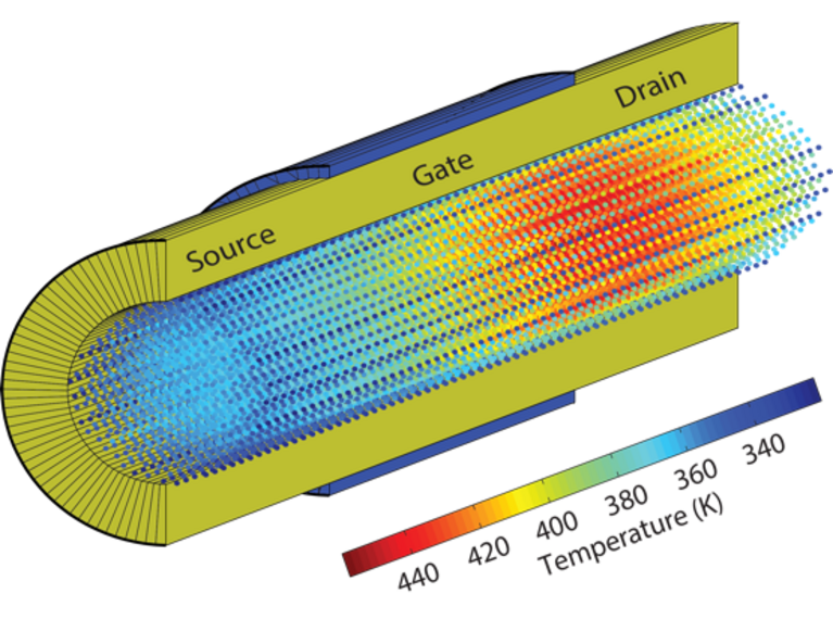
One problem when billions of conventional transistors are placed on one chip is that they generate a huge amount of heat and easily overheat. This is because the electrons release energy on their way through the transistor. Luisier and his team use their software OMEN – a so-called quantum simulator – to simulate the electron transport at atomic level in order to study exactly what happens. The simulated transistor consists of a nanowire made of silicon crystals. “When the electrons flow through the wire, they initially possess a constant, high amount of energy, which gradually decreases and is absorbed by the silicon’s crystal lattice in the form of so-called phonons,” explains Luisier. The interaction between the electrons and phonons heats the crystal and the overall energy remains intact – evidence for the researchers that their model reproduces the process correctly. The goal now is to construct the transistor based on the results obtained via the simulations in such a way that the electrons lose as little energy as possible along the way.
Playing with crystals
On the one hand, the researchers are able to “play” with the order of different crystal levels in the crystal and alter the crystal structure or replace silicon with another semiconductor material in their simulations. On the other hand, they can check the functionalities and different properties of the crystals simulated. For instance, the researchers simulated a nanowire, where the channel is encased in an oxide and a metallic contact (gate). The phonons emitted by the electrons are effectively “captured” in the channel and can only leave the structure at certain points – the beginning and end of the nanowire. “Replacing the shell around the wire with a structure that resembles the letter omega yields a larger area for the phonons to escape from,” says Luisier. If the area is also directly in contact with a cooling segment, the transistor heats up to a lesser extent. The semiconductors would also generate less heat if they were constructed from materials such as indium gallium arsenide or germanium because these materials enable the electrons to move through faster. However, they are much more expensive than silicon.
During the simulations, the researchers produce the structures designed atom by atom. Like in the conventional so-called “ab initio” method, which is used intensively to analyse the properties of materials, the Schrödinger Equation is also solved in the simulations conducted by Luisier’s team. This enables them to study how electrons and phonons interact.
However, there are two main differences: while the ab initio method solves the electrons’ wave movement in a closed or periodically repetitive system, Luisier’s group supplements the method with open boundary conditions, which enables transport to be simulated. The scientists can then observe both the electron flows and the thermal currents, and describe the interconnection with the surroundings, the interplay of the electron flow with the thermal currents. Another difference is that the calculations using OMEN are currently conducted based on empirical models as they are still too complex and more computer-intensive “ab initio”.
High-performance computing
However, new algorithms are being developed in a collaborative PASC project with scientists from the Università della Svizzera italiana and EPF Lausanne to render the calculations more efficient. “In the medium term, we want to replace all empirical models with ab initio ones so that we can calculate structures made of different materials more easily and accurately,” says Luisier. “This is why we need optimised algorithms and machines like Piz Daint.”
Nonetheless, Luisier stresses that, to the best of his knowledge, his team’s empirical approach is more state of the art than ever before in the development of electronic nanocomponents. Another of his group’s research focuses is the simulation of lithium ion batteries. “If we understand heat development in transistors or batteries more precisely, we will be able to propose better designs,” says Luisier. “OMEN is a component simulator of the new generation, where engineers use concepts that have never been used before in materials science, chemistry or physics.”
